01
Higher voltage capability
The wide bandgap gives 4H-SiC a critical electric field roughly ten times that of silicon in typical comparisons, enabling compact high-voltage device structures.
4H-SiC substrate systems
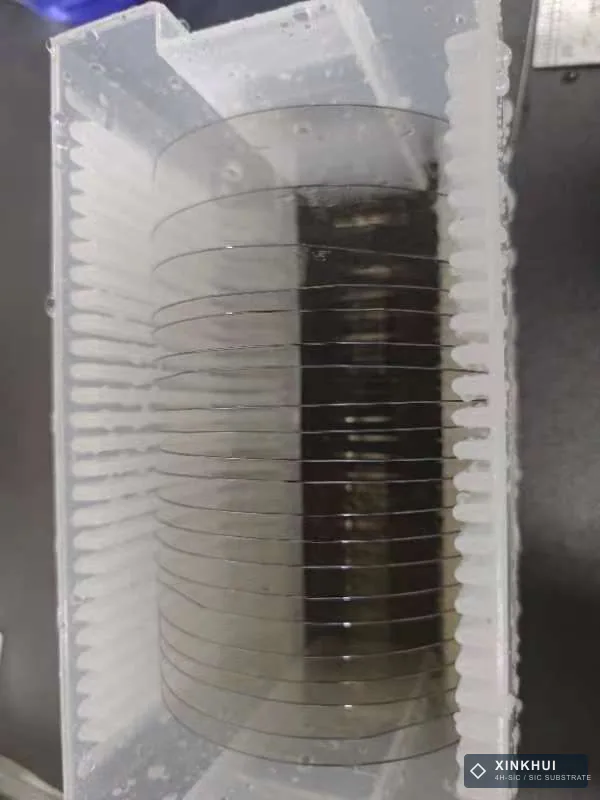
Production-grade HPSI silicon carbide wafers with precision CMP finishing, traceable inspection and a manufacturing route built around your device requirements.
Material intelligence
4H silicon carbide is a wide-bandgap semiconductor designed for demanding voltage, frequency and thermal conditions. Where conventional silicon reaches practical limits, 4H-SiC creates room for more compact, efficient and thermally resilient power systems.
4H-SiC is a single-crystal silicon carbide polytype with a bandgap of approximately 3.26 eV. It supports high-voltage power devices, RF and microwave components, and high-temperature electronics.
Why 4H-SiC
Use 4H-SiC when voltage, switching loss, thermal load or system volume materially affect the design. The benefit is system-level, not just a better material datasheet.
The wide bandgap gives 4H-SiC a critical electric field roughly ten times that of silicon in typical comparisons, enabling compact high-voltage device structures.
Fast switching and low reverse recovery can reduce conversion losses, especially when converter frequency and power density are rising.
High thermal conductivity can ease cooling requirements and improve thermal margins in densely packaged power modules and RF systems.
Better switching and thermal behavior can support fewer parallel devices, smaller filters and lower cooling burden in the right converter design.
The material remains dimensionally and chemically stable at elevated temperatures, helping device designers extend operating envelopes.
Xinkehui’s reference grade uses CMP on both faces, with roughness, bow and warp controlled for repeatable downstream processing.
About Xinkehui
Shanghai Xinkehui New Material Co., Ltd. is a high-tech enterprise engaged in the research, production, processing and sale of semiconductor substrates and optical crystal materials. The team combines crystal-material knowledge with precision processing, inspection and non-standard manufacturing.
Xinkehui serves customers in semiconductor, optical electronics, consumer electronics, optical communication and defense-related research, with products supplied to more than 20 countries and regions. The portfolio extends beyond SiC to sapphire, GaAs, InP, silicon, SOI, GaN, quartz glass and custom optical components.
Scope, certificate number and validity are confirmed against the relevant product and order.
Custom manufacturing
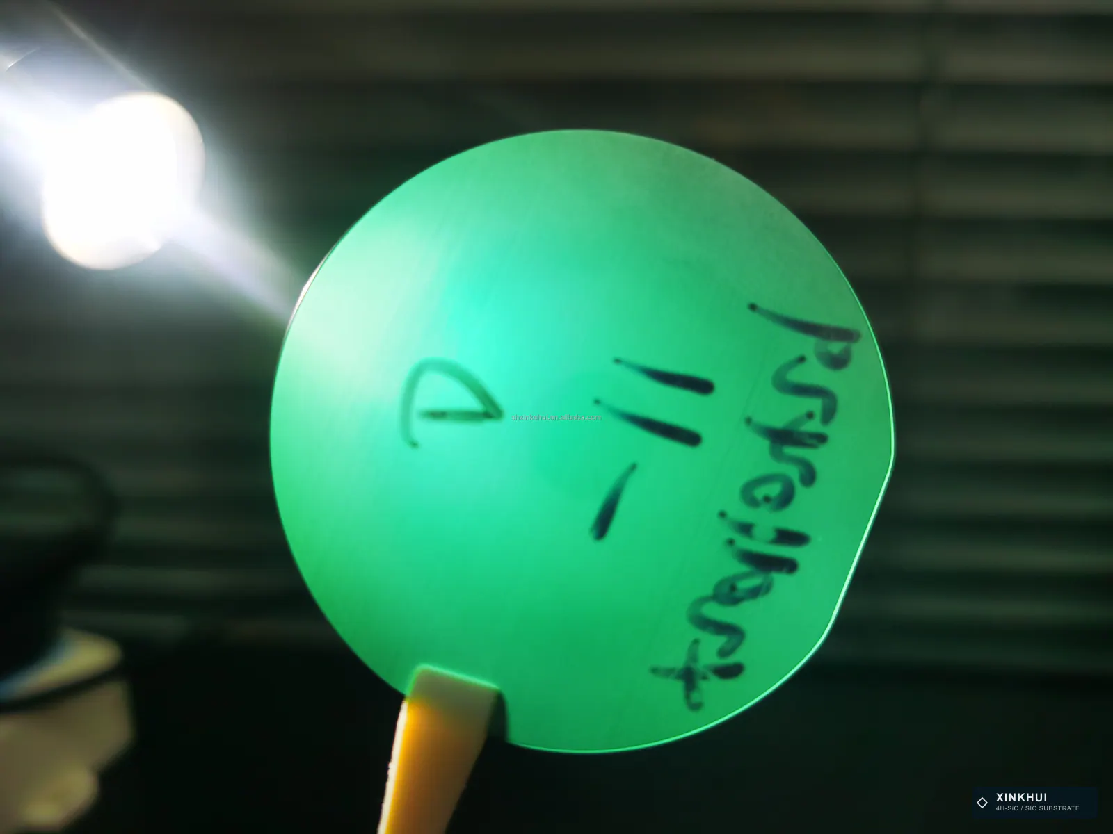
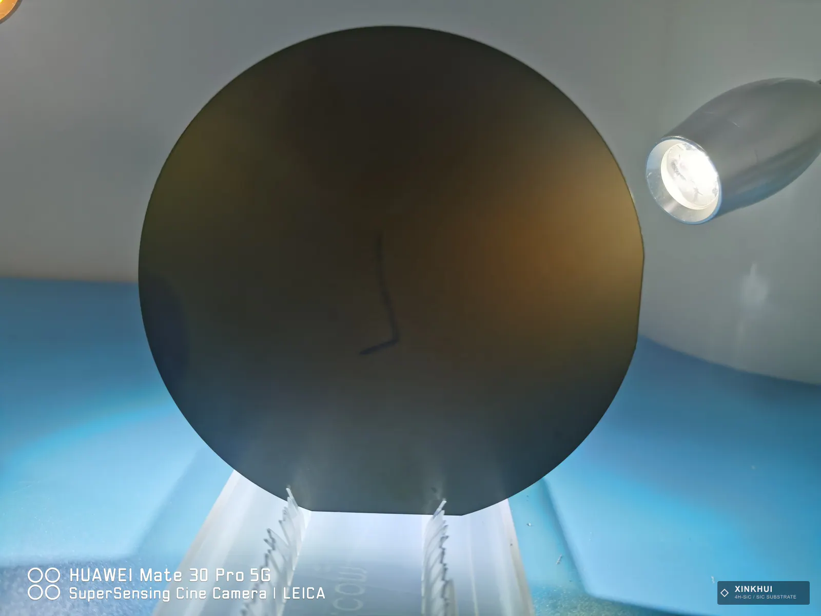
Diameter, thickness, off-axis angle, flat or notch, surface finish, grade and packaging can all be reviewed as one manufacturing requirement. Share a drawing, target values and the downstream process; Xinkehui will convert that into a practical production and inspection plan.
Device type, voltage class, epitaxial process and performance priorities.
Geometry, grade, orientation, finish, defects and acceptance criteria.
Processing sequence, inspection points, packing and release documentation.
Controlled processing with measurement against the approved requirement.
Applications
SiC is valuable where efficiency, thermal margin and power density matter together. Final material grade and device design should always be matched to the electrical and process requirements.
Traction inverters, onboard chargers, DC-DC converters and fast-charging power stages.
High-voltage powerSolar inverters, wind converters, battery systems and grid-connected energy storage.
Efficient conversionMotor drives, welding equipment, induction heating, UPS systems and power supplies.
Reliable duty cyclesTraction converters and auxiliary power systems that need compact, high-efficiency switching.
Robust power controlMicrowave devices, RF front ends, radar and satellite communication development.
HPSI isolationAerospace, defense and sensor systems exposed to thermal and environmental stress.
Thermal resilienceCompact fast chargers, server power, telecom power and high-density adapters.
Power densityMaterial evaluation, epitaxial development, device prototyping and pilot production.
Process developmentReference specification
The values below summarize the supplied reference configuration. Production acceptance criteria are frozen in the quotation, drawing and approved inspection plan.
| Parameter | Reference value | Practical meaning |
|---|---|---|
| Material | 4H-SiC | Wide-bandgap silicon carbide polytype |
| Grade / type | Production Grade / HPSI | High-purity semi-insulating reference grade |
| Diameter | 4 in / 99.5–100 mm | Wafer format for downstream device processing |
| Thickness | 500 ± 25 µm | Nominal substrate thickness |
| Crystal orientation | <0001> | Reference crystal-axis orientation |
| Off-axis orientation | 0 ± 0.2° | Specified angular tolerance |
| Surface | Si-face CMP / C-face CMP | Chemical-mechanical polished faces |
| Roughness | Ra ≤ 0.2 nm | Controlled surface finish |
| Resistivity | ≥ 1 × 10¹⁰ Ω·cm | High-purity semi-insulating behavior |
| FWHM | ≤ 45 arcsec | Crystal-quality X-ray rocking-curve reference |
| Bow | ≤ 5 µm | Controlled centerline curvature |
| Warp | ≤ 12 µm | Maximum deviation across the wafer reference plane |
| Micropipe density | ≤ 0.25 ea/cm² | Crystal-defect acceptance reference |
| Packaging | Nitrogen-filled / vacuum-sealed | Protective shipment configuration |
Other diameters, grades, custom thicknesses, surface treatments and packaging can be evaluated against your process requirements.
Material selection
Silicon remains an excellent, mature choice for many designs. 4H-SiC becomes compelling when conversion efficiency, voltage, temperature or system volume create a real design constraint.
| Design factor | 4H-SiC | Silicon |
|---|---|---|
| Bandgap | ~3.26 eV | ~1.12 eV |
| Critical field | ~10× silicon | Lower blocking-field capability |
| Thermal conductivity | ~4.9 W/cm·K | ~1.5 W/cm·K |
| High-voltage switching | Strong fit | More device and thermal overhead |
| System size and cooling | Potential reduction | Often a limiting consideration |
| Mature low-cost ecosystems | More specialized supply chain | Extensive maturity |
Values are order-of-magnitude material references, not device guarantees. Actual performance depends on device architecture, drivers, packaging, thermal design and operating conditions.
Manufacturing control
A controlled substrate is more than a polished surface. Crystal quality, geometry, finishing, cleanliness, inspection and packaging all influence the downstream process.
Material grade, crystal orientation, off-axis angle and target application are aligned before processing.
Wafer geometry and cutting route are planned around diameter, thickness and edge configuration.
Progressive material removal prepares the surface while controlling flatness, roughness and subsurface quality.
Dimensional, surface and specified material checks are completed before a controlled cleaning sequence.
Wafers are traceably identified, protected in carriers and packed in nitrogen-filled or vacuum-sealed packaging.
Inside Xinkehui
Engineering support, precision processing and inspection equipment work together around the customer’s final application.
Visit Xinkehui
Meet the engineering and commercial team in Shanghai, or arrange a technical discussion around your sample, drawing and process requirements. Visits are coordinated in advance so the right specialists are available.
Arrange a visit
Service and support
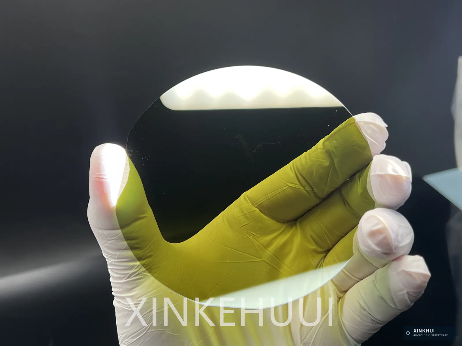
From sample review to shipment and nonconformance handling, the commercial terms are kept clear and tied to the approved specification.
Sample evaluation can be offered free of charge for qualified engineering applications, subject to specification and availability.
Confirmed material or specification nonconformance receives replacement or return review under the agreed order terms.
Freight support is available and may be included in a quoted order. Final shipping terms are confirmed in writing.
Nitrogen-filled or vacuum-sealed packing, wafer carriers and outer protection are selected for the shipment route.
Send the order reference, affected material and inspection information.
The team compares the evidence with the approved specification and handling record.
Replacement, return or corrective action is confirmed under the order terms.
Technical FAQ
Clear answers on material grade, wafer finishing, inspection, samples and order terms.
4H-SiC is a hexagonal silicon carbide crystal polytype with a wide bandgap of approximately 3.26 eV. Its high critical electric field, thermal conductivity and temperature tolerance make it useful for power electronic devices that must switch efficiently at high voltage.
HPSI 4H-SiC is designed for applications where low free-carrier absorption and controlled electrical isolation are important. It is commonly used in RF, microwave and optoelectronic device development. The required resistivity, orientation and surface specification should be matched to the epitaxial or device process.
The reference specification lists a 99.5–100 mm diameter, 500 ± 25 µm thickness, <0001> orientation, 0 ± 0.2° off-axis orientation, Si- and C-face CMP, Ra at or below 0.2 nm, resistivity of at least 1 × 10¹⁰ Ω·cm, FWHM at or below 45 arcsec, bow at or below 5 µm, warp at or below 12 µm, and micropipe density at or below 0.25 per square centimeter.
Yes, customization can be reviewed for diameter, thickness, off-axis angle, flat or notch configuration, surface preparation, polishing, grade and packaging. Send the target specification and the intended application so engineering can confirm technical and commercial feasibility.
Surface quality is generally supported by roughness, flatness, bow, warp, visual inspection, defect inspection and process-specific checks. The reference 4H-SiC grade uses a CMP surface with Ra at or below 0.2 nm. Final inspection criteria should be agreed before production.
Micropipes are hollow core defects that can affect epitaxial quality and device yield. A defined micropipe density provides an inspection and acceptance basis, but the required threshold depends on the device area and process sensitivity.
Inspection and traceability requirements can be agreed in the quotation and purchase specification. Depending on the order, documentation may cover lot identification, dimensional results, surface inspection and the applicable measurements stated in the approved specification.
Minimum quantity and lead time depend on the wafer grade, diameter, processing route, drawing requirements and current production schedule. Xinkehui confirms both after reviewing the technical requirement rather than using a universal estimate.
Complimentary sample evaluation may be available for qualified engineering applications, subject to specification, availability and approval. Share the intended process, required grade and quantity so the team can recommend an evaluation route.
Reference packaging is nitrogen-filled or vacuum-sealed. A typical shipment also uses wafer carriers and outer protective packaging selected for the destination and shipping method. Special labels, moisture protection and customer-specific packaging can be reviewed.
Documentation is confirmed with each quotation. Xinkehui can discuss inspection records, packaging information, lot identification and applicable quality documents. Company credentials include High-Tech Enterprise recognition, invention patents, CE and ISO certification; the relevant scope and validity should be confirmed for the order.
Yes. HPSI material is generally associated with RF, microwave and isolation-sensitive uses, while conductive grades are more common for power devices. Device architecture, epitaxial process, resistivity and defect requirements should drive the final selection.
Contact Xinkehui with the lot information and inspection evidence. Confirmed material or specification nonconformance is eligible for replacement or return review under the agreed order terms. Handling, storage and inspection conditions may form part of that review.
Start a conversation
Tell us the wafer diameter, grade, thickness, surface requirement and what you are building. We’ll use that information to recommend a practical material route.
Useful first response. Include a drawing or target values where possible so the reply can be technical, not generic.
Fields marked * are required.